
LED display industry development so far, including COB display, has emerged a variety of production packaging technology. From the previous lamp process, to table paste (SMD) process, to the emergence of COB packaging technology, and finally to the emergence of GOB packaging technology.
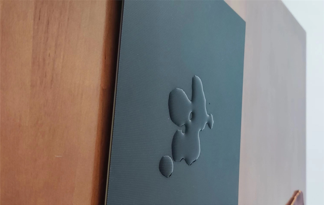
SMD: surface mounted devices. Surface mounted devices. led products packaged with SMD(table sticker technology) are lamp cups, supports, crystal cells, leads, epoxy resins and other materials encapsulated into different specifications of lamp beads. The lamp bead is welded on the circuit board by high temperature reflow welding with high speed SMT machine, and the display unit with different spacing is made. However, due to the existence of serious defects, it is unable to meet the current market demand. COB package, called chips on board, is a technology to solve the problem of led heat dissipation. Compared with in-line and SMD, it is characterized by space saving, simplified packaging and efficient thermal management. GOB, the abbreviation of glue on board, is an encapsulation technology designed to solve the protection problem of led light. It adopts an advanced new transparent material to encapsulate the substrate and its led packaging unit to form effective protection. The material is not only super transparent, but also has super thermal conductivity. GOB small spacing can adapt to any harsh environment, to achieve true moisture-proof, waterproof, dust-proof, anti-impact, anti-UV and other characteristics; GOB display products are generally aged for 72 hours after assembly and before gluing, and the lamp is tested. After gluing, aging for another 24 hours to confirm product quality again.
Generally, COB or GOB packaging is to encapsulate transparent packaging materials on COB or GOB modules by way of molding or gluing, complete the encapsulation of the whole module, form the encapsulation protection of point light source, and form a transparent optical path. The surface of the whole module is a mirror transparent body, without concentrating or astigmatism treatment on the surface of the module. The point light source inside the package body is transparent, so there will be crosstalk light between the point light source. Meanwhile, because the optical medium between the transparent package body and the surface air is different, the refractive index of the transparent package body is greater than that of the air. In this way, there will be total reflection of light on the interface between the package body and the air, and some light will return to the inside of the package body and be lost. In this way, cross-talk based on the above light and optical problems reflected back to the package will cause a great waste of light, and lead to a significant reduction of led COB/GOB display module contrast. In addition, there will be optical path difference between modules due to errors in the molding process between different modules in the molding packaging mode, which will result in visual color difference between different COB/GOB modules. As a result, led display assembled by COB/GOB will have serious visual color difference when the screen is black and lack of contrast when the screen is displayed, which will affect the display effect of the whole screen. Especially for the small pitch HD display, this poor visual performance has been particularly serious.
Post time: Dec-21-2022


